


スピントロニクスの基礎
Introduction to Spintronics
スピントロニクスは、1980年代後半の巨大磁気抵抗効果(GMR)により始まりました. GMRの発見者であるAlbert Fert・Peter Grünberg両博士は2007年にノーベル物理学賞を授与されました. GMRはスピン偏極電子が(反)平行配列した強磁性体磁化界面で散乱される頻度の差によって生じます. GMRは磁気記録の読み出しヘッドとして発見から10年程度で実用化され、後述するTMRヘッドに置き換えられたものの、その重要性は今でも色あせていません. Spintronics has been inspired by the discovery of giant magnetoresistance (GMR) late 1980s, which has been awarded by the Nobel Prize in physics in 2007. The GMR is based on the difference in resistance induced by spin-polarised conduction electron scattering at the interfaces of a ferromagnet/non-magnet/ferromagnet sandwich structure with respect to parallel and anti-parallel magnetisation configurations. This effect has been exploited in a read head in a hard disc drive (HDD), the most common data storage nowadays.
第2の重要な発見は、1995年の室温トンネル磁気抵抗効果(TMR)発見です. これはトンネル障壁を介した強磁性体間のスピン偏極電子トンネルに依る現象です. TMRはGMRに比べて1桁大きな比を示し、磁気記録におけるノイズ信号比を大幅に改善し、記録密度の向上に大きく貢献しました. The second major progress is the observation of tunneling magnetoresistance (TMR) at room temperature (RT) in 1995, derived from spin-dependent electron tunneling through an oxide barrier, which has been replaced with the non-magnetic layer in the GMR systems. The TMR offers a much larger MR ratio between the parallel and anti-parallel resistances, improving a signal to noise ratio for a higher areal density in a HDD.
これら磁気抵抗効果の発見と並行して、磁性材料開発もスピントロニクス発展に寄与してきました. 近年の真空技術向上に伴って、超高真空での成膜により欠陥の極めて少ない強磁性・非磁性薄膜をエピタキシャル(もしくは高配向)積層することが可能となりました. その結果、界面の平滑性などが向上しスピン非依存散乱を抑制することができ、TMR比をはじめとして大きく特性が向上しています. In concurrent with these magnetoelectronic discoveries, materials science has also contributed to the rapid development of spintronics. On account of recent advance in vacuum technology, these films, not only ferromagnetic films but also non-magnet including oxides, are able to be grown epitaxially, which has further improved the magnetic properties, such as the TMR ratios.
さらに微細加工技術の向上も素子作製に大きな役割を担ってきました. 例えば面内・面直接合におけるエッジなどの円滑化によるスピン非依存散乱の低減や、擬1次元伝導の実現などが挙げられます. さらに微細化に伴う原子レベルでの配列制御を通じて、新奇磁性材料(ハーフメタル強磁性体)の開発も進められており、100%スピン分極率や高磁気異方性、低ダンピング定数などが研究されています. Nano-fabrication is another key to broaden the spintronic device applications. Reduction in the junction area restricts the spin transport path into pseudo-1-dimensional pillar or wire, and also eliminates unfavorable defects at the junction interfaces, such as pinholes. Further reduction in size, even with precise atomic structure control, leads to creation of new spintronic materials (half-metallic ferromagnets), which confers unique magnetic characteristics, 100% spin polarisation and large magnetic anisotropy for instance.
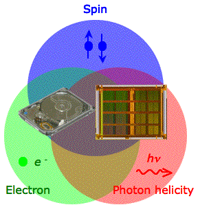 こうした様々な要素技術を組み合わせることによって、スピン・電子・光子などを幅広く利用した素子開発が進められています. 例えば光励起高速磁化反転やトポロジーを用いた材料などです. これらは消費電力が小さく動作速度も速いことから、次世代論理メモリ回路への応用が見込まれます.
Combination of the above nanoelectronics and materials science affords a platform for spintronics, where spins, electrons and photons interact with each other, realising spin-polarised electron transport, very large spin polarisation and photo-induced spin dynamics, etc. The integration of these three fundamental particles will promote future spintronic applications, a polarisation-tunable spin source, a spin transistor, spin diode and so on, each of which is anticipated to incorporate many accessible functionalities in conventional electronics.
こうした様々な要素技術を組み合わせることによって、スピン・電子・光子などを幅広く利用した素子開発が進められています. 例えば光励起高速磁化反転やトポロジーを用いた材料などです. これらは消費電力が小さく動作速度も速いことから、次世代論理メモリ回路への応用が見込まれます.
Combination of the above nanoelectronics and materials science affords a platform for spintronics, where spins, electrons and photons interact with each other, realising spin-polarised electron transport, very large spin polarisation and photo-induced spin dynamics, etc. The integration of these three fundamental particles will promote future spintronic applications, a polarisation-tunable spin source, a spin transistor, spin diode and so on, each of which is anticipated to incorporate many accessible functionalities in conventional electronics.
さらに興味のある方はFor further reading