最終更新日:2025年3月28日
Last updated: 28/03/2025
研究内容
Research
 我々の最終目標はスピントロニクスをつかって3端子トランジスタ・スイッチを作ることです. そのためには解決しなければいけない課題がいくつかあります: 非磁性体中のスピン流の制御、ホイスラー合金などを用いた100%スピン分極した材料の開発などです. 前者はナノスケールでの微細加工と擬1次元的な電子伝導の実現が必要となり、後者では原子レベルでの結晶配列制御が必須です. これらはトップダウンとボトムアップ手法に対応し、電子線描画・ミリング・フォトリソグラフィーや超高真空での成膜など多くの技術を利用しなければなりません.
The final goal of our research is to fabricate a spintronic three-terminal operator by investigating two major subjects: manipulation of a spin-polarised electron current in non-magnetic semiconductor/metal and realisation of perfect spin polarisation in a Heusler alloy film, both of which require nano-fabrication. In particular, the former subject has been investigated by electrically measuring spin transport properties in pseudo-1-dimensional structures, a nano-pillar or a nano-wire. These 1D structures have been fabricated with the "reductive" techniques, consisting of electron-beam nano-patterning and ion-beam etching onto a high quality multilayer. For the latter study to achieve perfect spin polarisation at room temperature, "constructive" methods have been employed for pseudo-2D film growth with precise atomic-scale control.
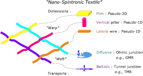 これらナノスケール・原子レベルの素子・材料に対して、電子伝導特性を精査することでスピン状態の安定性や付随する現象を左図のように研究しています. 例えば拡散伝導を測定することでフェルミ面EF近傍の電子状態を調べることができ、巨大磁気抵抗降下 (GMR)などを使った素子が実現されます. よりエネルギーが高い(>EF)弾道伝導の場合には、トンネル磁気抵抗効果 (TMR)への応用が期待されます.
By combining these nano-scale dimensions with two distinct spin-polarised electron transprt, ohmic and ballistic, both physics of the spin transport phenomena and spintronic device applications have been systematically studied as shown in the left figure. For the ohmic transport, spin-polarised electrons travel at the Fermi energy EF across a ferromagnet/non-magnetic metal junction for instance, showing giant magnetoresistance (GMR). For the ballistic transport, on the other hand, electron spins hold higher energy (>EF), such as through a tunnel barrier for tunneling magnetoresistance (TMR).